-
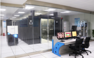
EDA software is a necessary tool for IC enterprise design. More than 30 kinds of tools are needed to complete a chip design, which is expensive. In order to solve the common needs of integrated circuit design enterprises in Jiangbei new area and reduce the R & D cost, EDA services have formed server computing power, EDA software time sharing, hardware simulation acceleration, EDA hybrid cloud, it / CAD environment construction, etc., to serve all aspects of enterprise R & D stage in the park.
-
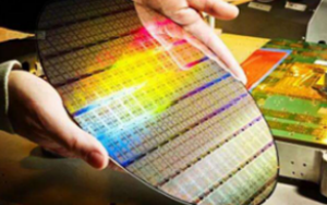
In order to meet the needs of enterprises to obtain advanced, preferential and fast streaming services, ICISC film services, together with international mainstream foundry, film channel enterprises and other partners, has established a channel platform covering the global mainstream process lines. The chip flow covers the process range of 12 nanometers and above, providing "one-stop Global streaming channel service" for chip enterprises Enterprise R & D. Contact: Mr.Sun 18813139658
-

Combined with the development trend of industry application, the construction of a leading special testing laboratory. At the same time to create from design verification, wafer testing and finished product testing and other types of professional services. At present, the common Shared laboratory, CP test laboratory, several special test laboratories and mass production wafer test center have been built in the design and verification stage. And open up the cooperation test resource sharing channel of nanjing university laboratory. Contact: Mr.Chen 13182919788
-

For the rapid development of service SoC chip design enterprises, ICisC IP Service takes the lead in building a global IP resource platform, integrating IP core resources at home and abroad, and entrusting a third-party professional operation team to provide professional IP technical services. To provide enterprises with IP sharing pool, IP normative certification, IP selection evaluation and IP customization development and other one-stop services.

